 ,
, Interactive Control Systems Tools
Phase Lag Compensator
The lag compensator reduces the gain of the system and adds phase lag. This is done either to increase the phase margin or to lower the closed loop bandwidth. The method for design of lag compensator shown here is based on Bode plots.
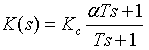
It is common to parametrize the compensator for Bode design as
, ![]()
In the Bode design we first choose the gain to satisfy the steady state error requirements. This is an advantage of the Bode plots based designs where the steady state error specifications can easily be met.
Then we find the other two parameters to meet the required phase margin. Evaluation the compensator gain at infinity shows that the maximum reduction in gain is
![]()
It is also clear that at the frequency ![]() , there is a minimal phase contribution form the lag compensator. These facts lead to the following design procedure:
, there is a minimal phase contribution form the lag compensator. These facts lead to the following design procedure:
1) Determine the gain Kc to satisfy the steady state error requirement.
2) Draw Bode plots of KcG(s).
3) If the phase margin is insufficient, find the frequency at which the phase margin is satisfied (add 5 degrees for safety). This frequency will be the compensated gain crossover frequency.
4) Find the gain of KcG(s) at the compensated gain crossover frequency. This is the amount of gain that needs to be reduced by the compensator, i.e.
![]()
5) To minimize the phase contribution of the compensator, make

6) Draw Bode plots of the open loop system and confirm the design
7) Simulate the closed loop system.
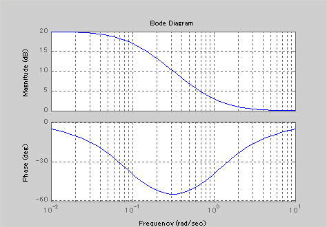
The Bode diagram of phase lag compensator is shown below.
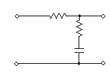
A simple realization of lag compensator is
Reference: