Interactive Control Systems Tools
Phase Lead Compensator
Here only the design based on Bode diagrams is briefly presented. For more information read the references given at the end of this description.
The basic idea in Bode design is to shape the open loop transfer function so that it will have desirable low frequency gain (for steady state error or disturbance rejection properties), desirable gain crossover frequency (for speed of response), and adequate stability margins. It is common to parametrize the compensator for Bode design as

In the Bode design we first choose the gain to satisfy the steady state error requirements. This is an advantage of the Bode plots based designs where the steady state error specifications can easily be met. Then we satisfy the phase margin requirements and try to achieve the desired crossover frequency. Introduce
![]()
where ![]() .
.
Let's calculate the phase contributed by this lead compensator:
![]()
Because we are using this method to achieve the desired phase margin, we are concerned with the amount of phase lead added by the compensator at the compensated crossover frequency. For easy design we try to add the maximum possible phase lead at the crossover frequency. The frequency at which the maximum phase lead occurs can be find by differentiating the above equation:

Then the maximum phase lead that can be achieved is:

And the following relationships follow directly:
![]()
The additional amplitude contributed by the compensator is:
![]()
Now we are ready to summarize the procedure for design of lead compensator:
1) Select Kc to achieve the required steady state error
2) Draw Bode plots for KcG(s), and determine the phase margin
3) Determine the additional phase lead required; this is the initial ![]() . Add a few degrees to the phase just determined to find the working
. Add a few degrees to the phase just determined to find the working ![]() .
.
4) Compute ![]() from the above relation.
from the above relation.
5) Find the frequency at which ![]() ; this frequency will be the compensated
; this frequency will be the compensated ![]() .
.
6) Compute T
7) Draw Bode plots of the open loop system to confirm the design.
8) Close the loop, and determine appropriate closed loop responses.
Note: Because the addition of the compensator zero will cause the compensated crossover frequency to increase. This increase will lead to smaller phase margin. Because of this in the above step (3) we add few degrees to obtain the desired phase margin.
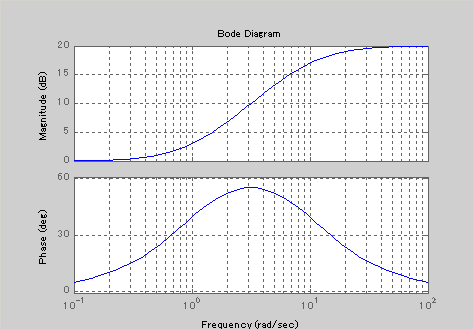
The Bode plots of lead compensator are shown below

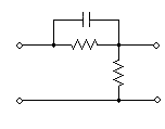
A simple realization of a phase lead compensator is shown below

Reference: